Importance of LED lighting in clean rooms and photolithography
The Importance of LED Lighting in Clean Rooms and Photolithography In the realm of advanced technology and precision manufacturing, clean rooms and photolithography play a crucial role in ensuring the quality and reliability of semiconductor devices and microelectronic components.
Clean rooms are controlled environments designed to minimize airborne particles, contaminants, and pollutants, while photolithography is a key process used in semiconductor fabrication to transfer patterns onto a substrate using light-sensitive materials.
Both clean rooms and photolithography require meticulous attention to detail and precision, making proper lighting essential for optimal performance.
A little about clean rooms
Clean rooms are classified based on the number of particles per cubic meter of air, with stricter classifications requiring lower particle counts. These controlled environments are essential for industries such as semiconductor manufacturing, pharmaceuticals, biotechnology, and aerospace, where even the tiniest particle can compromise product quality and performance.
Clean rooms feature specialized ventilation systems, air filtration, and strict protocols for personnel attire and behavior to maintain cleanliness.
What is Photolithography?
Photolithography is a fundamental process in semiconductor manufacturing, used to create intricate patterns on silicon wafers or other substrates. It involves several steps, including coating the substrate with a light-sensitive material called a photoresist, exposing it to light through a photomask or reticle containing the desired pattern, and developing the exposed photoresist to transfer the pattern onto the substrate.
Precise control of light intensity, wavelength, and uniformity is critical to achieving accurate pattern transfer and ensuring high yields in semiconductor fabrication.
The significance of proper lighting in clean rooms and photolithography
In both clean rooms and photolithography facilities, quality lighting is paramount for several reasons:
- Visibility and Clarity: Clean rooms require adequate illumination for personnel to perform tasks with precision and accuracy. Proper lighting ensures clear visibility of workstations, equipment, and instrumentation, reducing the risk of errors and improving productivity.
Similarly, in photolithography, precise control of light intensity and uniformity is essential for achieving accurate pattern transfer and minimizing defects in semiconductor devices. - Contamination Control: Clean rooms rely on lighting fixtures designed to minimize particle generation and electrostatic discharge (ESD) to maintain cleanliness.
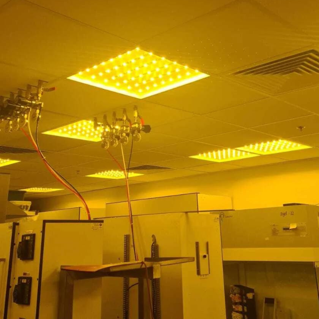
LED lighting, with its sealed and durable construction, produces minimal heat and eliminates the risk of contamination from broken bulbs or hazardous materials, making it ideal for clean room environments where cleanliness is paramount. - Color Rendering and Accuracy: Photolithography requires lighting sources with high color rendering index (CRI) to accurately represent colors and patterns during mask alignment and pattern inspection.
LED lighting offers excellent color rendering properties, allowing semiconductor manufacturers to achieve precise pattern transfer and ensure consistency in device performance. - Energy Efficiency and Sustainability: LED lighting consumes significantly less energy than traditional lighting sources, reducing electricity costs and environmental impact in clean room and photolithography applications. Furthermore, LED fixtures have longer lifespans and require less frequent replacement, minimizing downtime and maintenance costs in critical manufacturing environments.
In conclusion, the importance of quality lighting in clean rooms and photolithography cannot be overstated. Whether it's providing clear visibility for precision tasks, minimizing contamination risks, ensuring accurate pattern transfer, or promoting energy efficiency, LED lighting offers unparalleled benefits for industries reliant on clean and controlled environments.
By investing in advanced LED lighting solutions, semiconductor manufacturers and other high-tech industries can enhance productivity, improve product quality, and maintain competitive advantage in today's dynamic market landscape.
Interested in LED lighting for clean rooms or photolithography? You've come to the right place!
At Hannis Technologies, we have extensive experience in the design, manufacturing, and assembly of LED lighting for any purpose, with experience in clean room and photolithography development. Sound interesting to you? Contact us for more details.